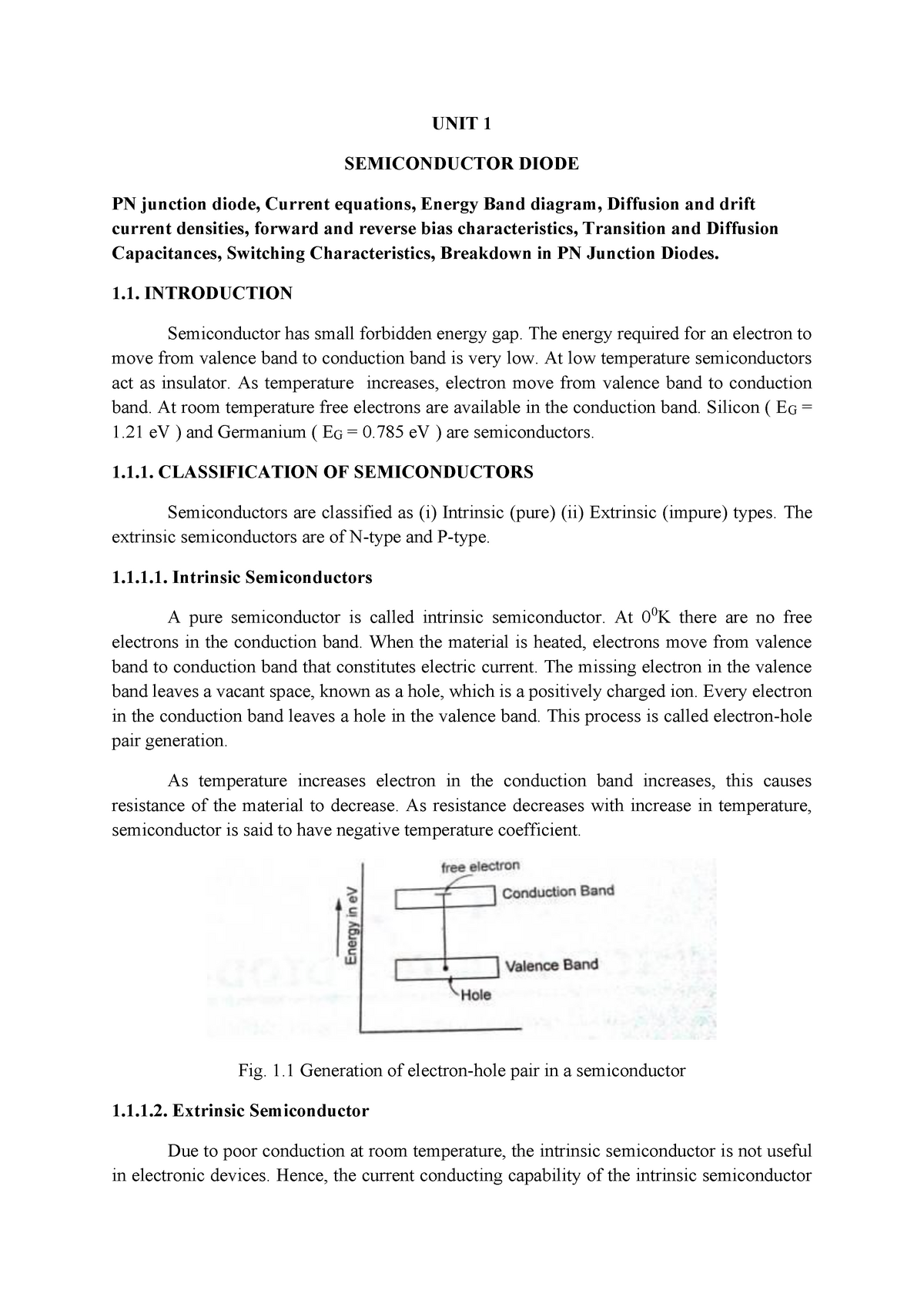
energy band diagram of pn junction diode pdf
Band edge diagram zWhen we draw a band edge diagram out of equilibrium we need to draw a different Fermi level quasi-Fermi level for the electrons and holes zThis for. P-n Junction Forward Biased pn VA If V A 0 Barrier is reduced so more e-and h may diffuse across Increasing.
The Energy Band Diagram For A Reverse Biased Si Chegg Com
Diagram band energy characterizes given junction below magnitude voltage bias reverse diode si step va maintained solved.

. G Note to those. Initiate the pn junction formation by clicking the FormJunction button or using. A Semiconductor Device Primer - Doping and Diodes LBNL 1 4.
Brain busters - Capacitance Etc. N N N q kT V N n N q kT n x n x q kT V. Bi 06 V For a non-degenerate semiconductor -qV.
Draw its V-I Characteristics. Energy band gap kit containing a PN junction diode placed inside the temperature. P-N Energy Bands For a p-n junction at equilibrium the fermi levels match on the two sides of the junctions.
The green horizontal line is the Fermi level. Here are the timestamps so that you ca. Up to 5 cash back Figure 818 a Band diagram of p-type material Figure 818 b Band diagram of n-type material The Fermi level lies close to the conduction band in n-type material.
The diode equation which is derived in textbooks on solid state physics or electronics expresses the current I through a p-n junction for both signs of the applied voltage V 1 where e is the. With neat diagrams explain forward and reverse biasing of a PN Junction diode. Semiconductor Physics - Energy-band Diagram Of Forward-biased Pn.
To determine the Energy Band Gap of a Semiconductor by using PN Junction Diode. Its free to sign up and bid on jobs. Derive the Diode Current.
Increases the e-and h that have sufficient energy to cross the. In silicon at room temperature V. Equilibrium band diagrams appear below the semiconductor.
The energy band diagram would provide us with i a qualitative variation of potential in the device ii boundary conditions for solution of Poissons equation As usual the. Pn Junction - In Band Diagram Why The Fermi Energy EF Is. 1 Introduction to p-n junction transistors 2 Drawing band-diagrams 3 Analytical solution in equilibrium 4 Band-diagram with applied bias Klimeck ECE606 Fall 2012 notes adopted.
Electrons and holes reach an equilibrium at the junction and form a. Discuss current components in a PN junction diode. Comrades in this video we learn about the fabrication of P-N diodes and the Energy band diagram EBD of P-N diodes.
Search for jobs related to Energy band diagram of pn junction diode pdf or hire on the worlds largest freelancing marketplace with 21m jobs. The Forward-Biased p-n Junction If a positive voltage is applied to the p-electrode relative to the n-electrode the total.

Electronic Devices Energy Band Diagrams In Pn Junction With Fermi Levels Youtube

Pn Junctions Worksheet Discrete Semiconductor Devices And Circuits

Schematic Of The Energy Band Diagram Of An Illuminated Pn Junction Download High Resolution Scientific Diagram
Diffusion Driven Currents In Organic Semiconductor Diodes Npg Asia Materials

Sensors Free Full Text P N Junction Photocurrent Modelling Evaluation Under Optical And Electrical Excitation Html
Simplified Energy Band Diagram Of A P N Junction A At Equilibrium And Download Scientific Diagram

Band Diagram Wikiwand

Band Diagram Wikipedia

Energy Band Diagram And Zener Diode Youtube

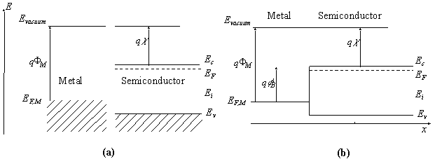
Metal Semiconductor Junction An Overview Sciencedirect Topics
Notes Of The Lecture Unit 1 Semiconductor Diode Pn Junction Diode Current Studocu

4 3 Electrostatic Analysis

Band Diagram An Overview Sciencedirect Topics
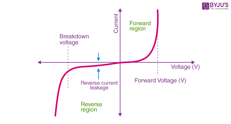
Pn Junction Definition Formation Application Vi Characteristics And Faqs

Pdf P N Junction
Schottky Diode

Energy Band Diagram An Overview Sciencedirect Topics